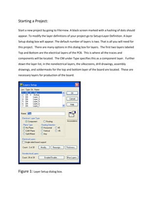
← Wiring Instructions for Craftsman Garage Door Opener: The DIY Fix Wiring diagram for craftsman garage door opener » wiring digital and Was Ist Ein Block Volleyball? The Game-Changing Move Explained What is a block in volleyball? mastering defense skills →
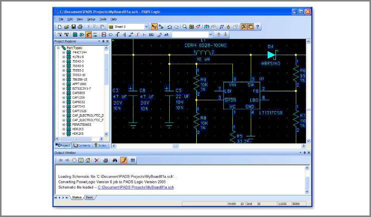
If you are looking for Day1 Basics of PCB Design in PADS | PDF | Printed Circuit Board | Design you've came to the right web. We have 25 Pictures about Day1 Basics of PCB Design in PADS | PDF | Printed Circuit Board | Design like PADS Tutorial For PCB Designing | PDF | Printed Circuit Board | Capacitor, Day1 Basics of PCB Design in PADS | PDF | Printed Circuit Board | Design and also PADS Layout Tutorial - SGI - PCB Design | PDF | Printed Circuit Board. Here you go:
Day1 Basics Of PCB Design In PADS | PDF | Printed Circuit Board | Design
 www.scribd.com
Day1 Basics of PCB Design in PADS | PDF | Printed Circuit Board | Design
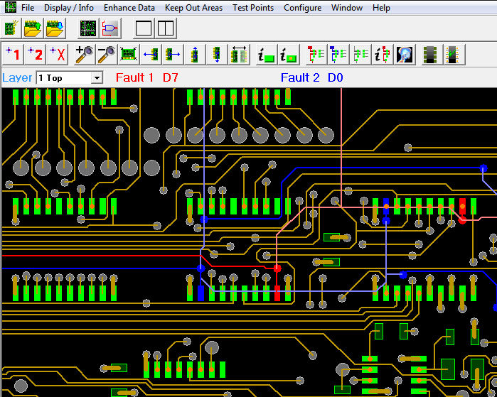
Nerdy Texts Of Analog And Embedded Systems Wizardry » PCB Layout
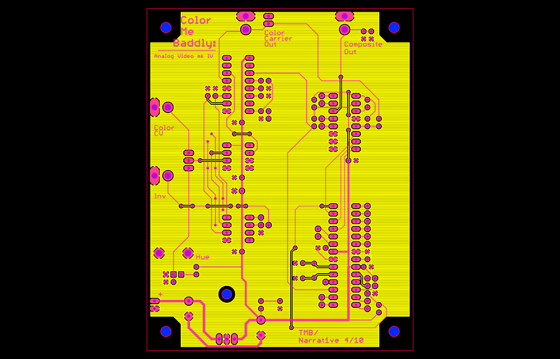 blog.narrat1ve.com
Nerdy Texts of Analog and Embedded Systems Wizardry » PCB Layout
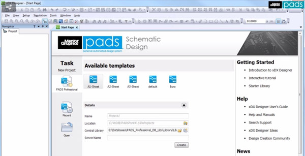
Siemens PCB Schematic Design | PADS Professional | Cadlog
 www.cadlog.com
Siemens PCB Schematic Design | PADS Professional | Cadlog
PADS PCB Design Tutorial For Beginners: A Step-by-Step Guide
 www.ourpcb.com
PADS PCB Design Tutorial for Beginners: A Step-by-Step Guide
PADS PCB Design Tutorial | PCBCart
 www.pcbcart.com
PADS PCB Design Tutorial | PCBCart
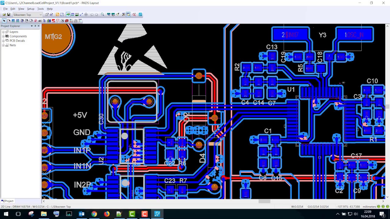
PCB Layout Design By Siemens | PADS Professional | Cadlog
 www.cadlog.com
PCB Layout Design by Siemens | PADS Professional | Cadlog
Siemens PCB Schematic Design | PADS Professional | Cadlog
 www.cadlog.com
Siemens PCB Schematic Design | PADS Professional | Cadlog
Pcb Design - PCB Layout. The Path Between Pads - Electrical Engineering
 electronics.stackexchange.com
pcb design - PCB Layout. The path between pads - Electrical Engineering ...
Pads PCB Designer: A Comprehensive Guide To PCB Designing – Hillman
 hillmancurtis.com
Pads PCB Designer: A Comprehensive Guide to PCB Designing – Hillman ...
Pads Layout Viewer Pcb Circuits
 www.fity.club
Pads Layout Viewer Pcb Circuits
PADS PCB Design Software – Krishwave
 krishwave.com
PADS PCB Design Software – krishwave
PCB Designing In PADS Layout | PDF | Computing | Technology & Computing
 www.slideshare.net
PCB designing in PADS layout | PDF | Computing | Technology & Computing
PADs PCB Design Services - Expert Solutions By 911EDA
 www.911eda.com
PADs PCB Design Services - Expert Solutions by 911EDA
Pads Layout Viewer Pcb Circuits
 www.fity.club
Pads Layout Viewer Pcb Circuits
PCB Designing In PADS Layout | PDF | Computing | Technology & Computing
 www.slideshare.net
PCB designing in PADS layout | PDF | Computing | Technology & Computing
Introduction To PCBs: Exploring Types, Features, And Applications
 www.rowsum.com
Introduction to PCBs: Exploring Types, Features, and Applications
Pads PCB Designer: A Comprehensive Guide To PCB Designing – Hillman
 hillmancurtis.com
Pads PCB Designer: A Comprehensive Guide to PCB Designing – Hillman ...
PADs PCB Design Services - Expert Solutions By 911EDA
 www.911eda.com
PADs PCB Design Services - Expert Solutions by 911EDA
Siemens PCB Schematic Design | PADS Professional | Cadlog
 www.cadlog.com
Siemens PCB Schematic Design | PADS Professional | Cadlog
PCB Designing In PADS Layout | PDF | Computing | Technology & Computing
 www.slideshare.net
PCB designing in PADS layout | PDF | Computing | Technology & Computing
PADS Layout Tutorial - SGI - PCB Design | PDF | Printed Circuit Board
 www.scribd.com
PADS Layout Tutorial - SGI - PCB Design | PDF | Printed Circuit Board ...
Pads Layout Viewer Pcb Circuits
 fity.club
Pads Layout Viewer Pcb Circuits
Siemens PCB Schematic Design | PADS Professional | Cadlog
 www.cadlog.com
Siemens PCB Schematic Design | PADS Professional | Cadlog
PCB Designing In PADS Layout
 www.slideshare.net
PCB designing in PADS layout
PADS Tutorial For PCB Designing | PDF | Printed Circuit Board | Capacitor
 www.scribd.com
PADS Tutorial For PCB Designing | PDF | Printed Circuit Board | Capacitor
Pcb design. Pcb designing in pads layout. Nerdy texts of analog and embedded systems wizardry » pcb layout